
PCB design for beginners can be difficult, but with the right procedures in place it becomes much easier. In this article, we show you how to do controlled impedance routing on your PCB.
How to do controlled impedance in PCB design:
Printed circuit boards are integral in many electronic products; thus, it is important to know how to design them with controlled impedance. By following the six steps listed in this blog post, you can make sure that your PCB has properlycontrolled impedance. If you want to learn more about designing PCBs or other aspects of electronic product development, enroll in our training programs. Our experts will be able teach you everything need to know in order to develop high-quality electronics.
How to do controlled impedance in PCB design:
First: What is controlled impedance? It's a method used to keep the characteristic impedance of a PCB trace the same as much as possible to avoid signal reflections on said trace. If the impedance changes (e.g. branching off into two other traces, necking down too much, or suddenly opening to a wide copper pour), then it will cause signal reflections, which are bad business for signal integrity.
Now let's discuss a procedure to define and control the impedance of traces (whether single ended or differential).
1. Find out the impedance called for a communication protocol (e.g. 50Ω single ended or 90-100Ω differential, from datasheets, application notes, or that protocol's standard, e.g. PCIe, SPI, USB, etc.)
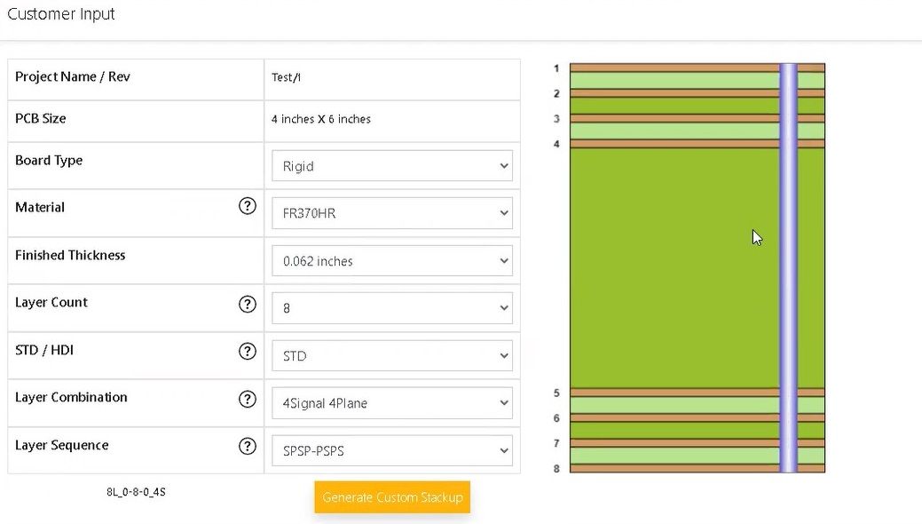
2. Talk to your PCB manufacturer to find out what materials and board stack-ups they actually do. The layers, dielectric materials, dielectric (Dk, ε_r), dissipation factors, minimum trace width, minimum spacing allowed, etc. These values affect signal propagation, attenuation, etc.
3. Learn how the H and E magnetic and electric fields behave when generated by signals on a printed circuit board. This will help you choose your stack-up plan. The plan/strategy, I talk about in a previous post.
4. With that stack-up planned, copper thicknesses defined and dielectrics, etc. use controlled impedance trace equations to generate the correct trace widths for your microstrip and stripline structures in the PCB. (keep current carrying capacity in mind as well)
Side note: An easier (and more common) way is to use software that automatically adjusts the traces for you based on your impedance requirements and the materials you've put into the stack-up.
5. See what values for trace widths pop out to hit your target impedances.
6. Double check these values with your manufacturer, set your rules and constraints, and you're ready to start routing with controlled impedance!
If you would like to test out a free PCB stack-up designer tool, check out Sierra Circuits, a California manufacturer setting the standard for PCB design tips, tools and guidelines.
To learn more about hardware and PCB design, follow us on LinkedIn.
Printed circuit boards are integral in many electronic products; thus, it is important to know how to design them with controlled impedance. By following the six steps listed in this blog post, you can make sure that your PCB has properlycontrolled impedance. If you want to learn more about designing PCBs or other aspects of electronic product development, enroll in our training programs. Our experts will be able teach you everything need to know in order to develop high-quality electronics.
If you're trying to become a 400% more confident, successful hardware engineer in 6 months or less, and secure your and your family's future in this shifting economy, Contact Us about our formal PCB Design Accelerator training program.
Created with